Département d'Optronique (LETI)
Laboratoire d'Imagerie thermique et THz
01-09-2021
SL-DRT-21-0313
Photonics, Imaging and displays (.pdf)
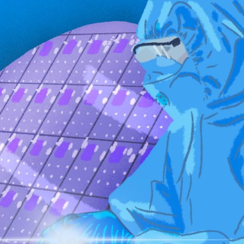
Uncooled thermal detectors absorb the infrared flux in wavelength range from 7µm to 14µm. This corresponds to an atmospheric transmission window and to the maximum emission of a blackbody at 300K, which enables to measure temperature variations of less than 100mK. The operating principle of microbolometers is based on the temperature measurement of a suspended membrane absorbing the infrared flux. The thermal transducer is the sensitive element of the microbolomčtre, which determines its signal-to-noise ratio and therefore the performance of the bolometric pixel. Most commercial microbolometers use a thermistor with amorphous silicon or vanadium oxide for its high temperature coefficient (TCR = 2-4% / K) and low flicker noise (1/f noise). The thesis proposal deals with a breakthrough technology for microbolometers. Unlike conventional thermistor detectors, the student will examine the use of SOI vertical diodes as transductor. The topic will focus on characterizing and modeling the performance of such a device.
Département d'Optronique (LETI)
Laboratoire des Capteurs Optiques
01-10-2020
SL-DRT-21-0315
Photonics, Imaging and displays (.pdf)
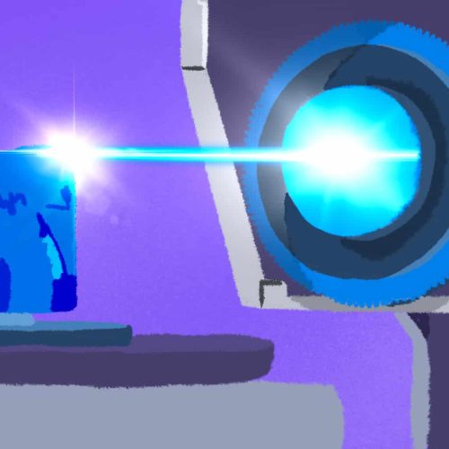
One of the main challenges for silicon photonics is an integrated laser technologically compatible with microelectronic foundries. Traditional, standalone semiconductor lasers use III-V semiconductors that are not accepted in the silicon foundries, contrary to the group-IV semiconductors. CEA Grenoble is among only few labs that already demonstrated mid-infrared optically pumped lasing in group-IV semiconductors, both in Ge and GeSn. With fully relaxed or tensile-strained heterostructures and quantum wells made of silicon-germanium-tin alloys (Si)GeSn, today we target continuous lasing at room temperature and efficient photodetectors in 200 mm wafers. To reach room temerature lasing, we need to improve the optical gain and optimize the carrier confinement. The improvements will require a redesign of the quantum wells and heterojunctions in germanium tin, through playing with atomic compositions and the mechanical strain at the micro-nanoscopic scale. Like the lasers we already demonstrated, the designed (Si)GeSn layers will be epitaxially grown at the main 200 mm CMOS fab facility of CEA Leti, and further fab-processed by the PhD candidate in smaller-scale clean rooms. Laser developments will be used to realize efficient GeSn photodetectors. The objectives of the research will be: (i) to reduce the number of crystalline defects in the GeSn gain regions, (ii) to design efficient (Si)GeSn stacks that confine both electrons and holes, while providing strong optical gain (iii) to apply and control tensile strain in germanium tin layers, (iv) to evaluate the optical gain under optical pumping and electrical injection, at different strains and doping levels, (v) to design and fabricate laser cavities with strong optical confinement (vi) to obtain germanium-based group-IV lasers that are tunable and lase continuously. (vii) to test fabricated devices (light sources and photodetectors) in gas detection cells On a longer term, such lasers will be widely used in ubiquitous miniaturized, low-power devices for optical gas sensing and environmental monitoring. This work will imply contacts with foreign labs working on the same vibrant topic.
Département d'Optronique (LETI)
Laboratoire des Composants Emissifs
01-10-2021
SL-DRT-21-0395
Photonics, Imaging and displays (.pdf)
The detection and manipulation of the polarized light is very attractive, in particular because of the interest in using circularly polarized light (LCP) in many areas of societal importance such as technologies display, information transmission, cryptography, bio-medical imaging or even the detection of chiral molecules of pharmaceutical interest. Due to their ability to interact specifically with an LCP and to modulate its polarization, chiral molecular materials stand out as an element of choice for exploring these innovative applications and considering new potential in organic electronics. In addition, the specific property of chiral molecules to induce electronic spin selectivity in the conduction of electric current (CISS effect for Chiral Induced Spin Selectivity) also opens up opportunities in the field of organic spintronics. Consequently, the synthesis of innovative pi conjugated chiral semiconductors, presenting an easy modulation of their physicochemical properties and the integration of these materials in optoelectronic devices of the OLEDs, OPDs or OFETs type is of interest both fundamental and 'application. The thesis project will be done in collaboration with a CNRS chemistry laboratory in Rennes, France, and the LCEM laboratory (at CEA / LETI, Grenoble, France) specialized in organic semiconductors. The objectives of the thesis student will be to synthesize new chiral organic charge transporters and to characterize their photophysical (absorption and emission) and opto-electronic properties. The most promising molecules will be integrated into OLEDs and OPDs devices. The photophysical synthesis and characterization part (circular dichroism spectrometer, non-polarized and circularly polarized luminescence spectrometer, PER, etc.) will be carried out at the CNRS chemistry laboratory. The integration of molecules in OLEDs and OPDs devices will be done in the LCEM laboratory where the deposition equipment (PVD chamber for organic materials) and the opto-electronic characterization means (IVL, C (V), TLM, Photocurrent, hall effect, etc.).
Département d'Optronique (LETI)
Laboratoire d'Imagerie sur Silicium
01-01-2021
SL-DRT-21-0477
Photonics, Imaging and displays (.pdf)
Advanced optoelectronic devices such as the single-photon avalanche diode (SPAD) are now widely employed in the fields of 3D imaging, camera assist, laser ranging and proximity. Next generation of SPAD will be devoted to time-of-flight 3D ranging and fast movement detection, notably for long LiDaR used in autonomous driving cars. The PhD work will consist in developing and exploiting home-made simulators for optoelectronic devices and more specifically, Ge separated absorption SPAD. In this type of sensors infrared light is absorbed in germanium and photogenerated carriers are transported into the silicon avalanche zone for signal amplification. A close understanding of the transport between the two materials is fundamental for optimization of the device. This will be done through simulation and calibrations of the models. First, process simulations of doping implantation, but also residual strain in the epitaxial Ge layer will be used to extract realistic doping profiles and hence inserted in the Monte Carlo (MC) code. Second, by using 3D particle MC simulation for solving the Boltzmann transport equation, the time behavior of different designs of Si- and Ge-based SPAD devices will be statistically analyzed in order to reduce the jitter and to enhance the photon detection probability. The MC technique is a unique tool to analyze single particle trajectories as well as the time evolution of terminal currents and voltages.
Département d'Optronique (LETI)
Laboratoire d'Intégration Photonique sur Silicium
01-10-2021
SL-DRT-21-0605
Photonics, Imaging and displays (.pdf)
Quantum information processing turns out to be a major challenge for our society with the development of quantum computers, able to solve complex problems much more rapidly than a classical computer, and of quantum communications providing absolute security for information transfer. The development of integrated technologies is essential for the future large-scale deployment of compact and low-cost quantum information systems. CEA-Leti has been developing for several years a silicon photonics platform, providing integrated components and circuits for various applications such as telecom/datacom, lidars and more recently quantum communications. The objective of this PhD is in a first step to design, fabricate in the Leti clean room and characterize a new generation of advanced superconducting quantum detectors on Silicon able to detect single photons with above 90% efficiency. In a second step, these detectors will be integrated into secure quantum communication circuits. This PhD will benefit from collaborations with academic laboratories in France and in Europe.