


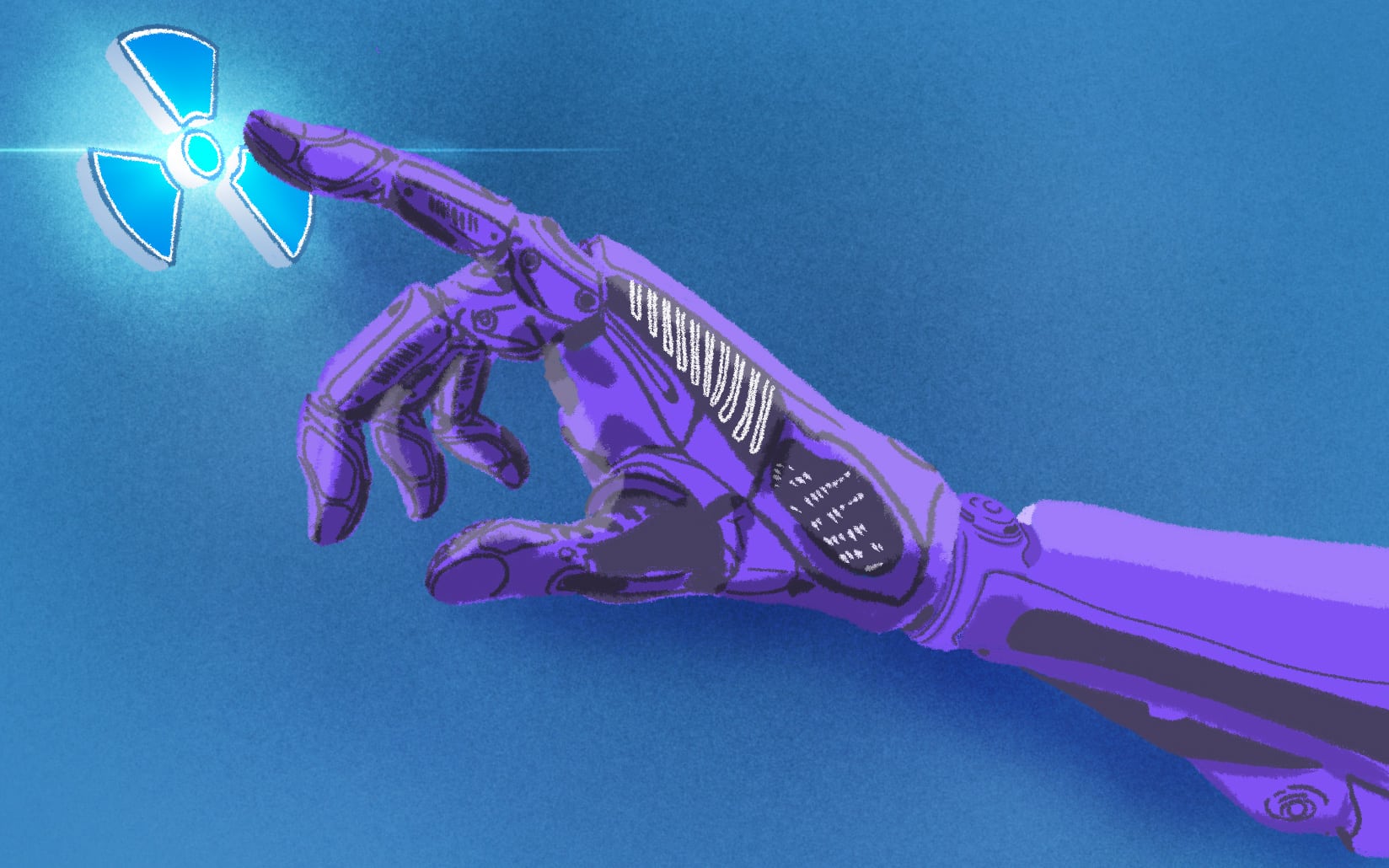


Work-study programmes at CEA - Our apprentices answer your questions
Read more »
The Technology Research Division's work-study recruitment campaign is underway! Every year, we recruit over 150 work-study students.
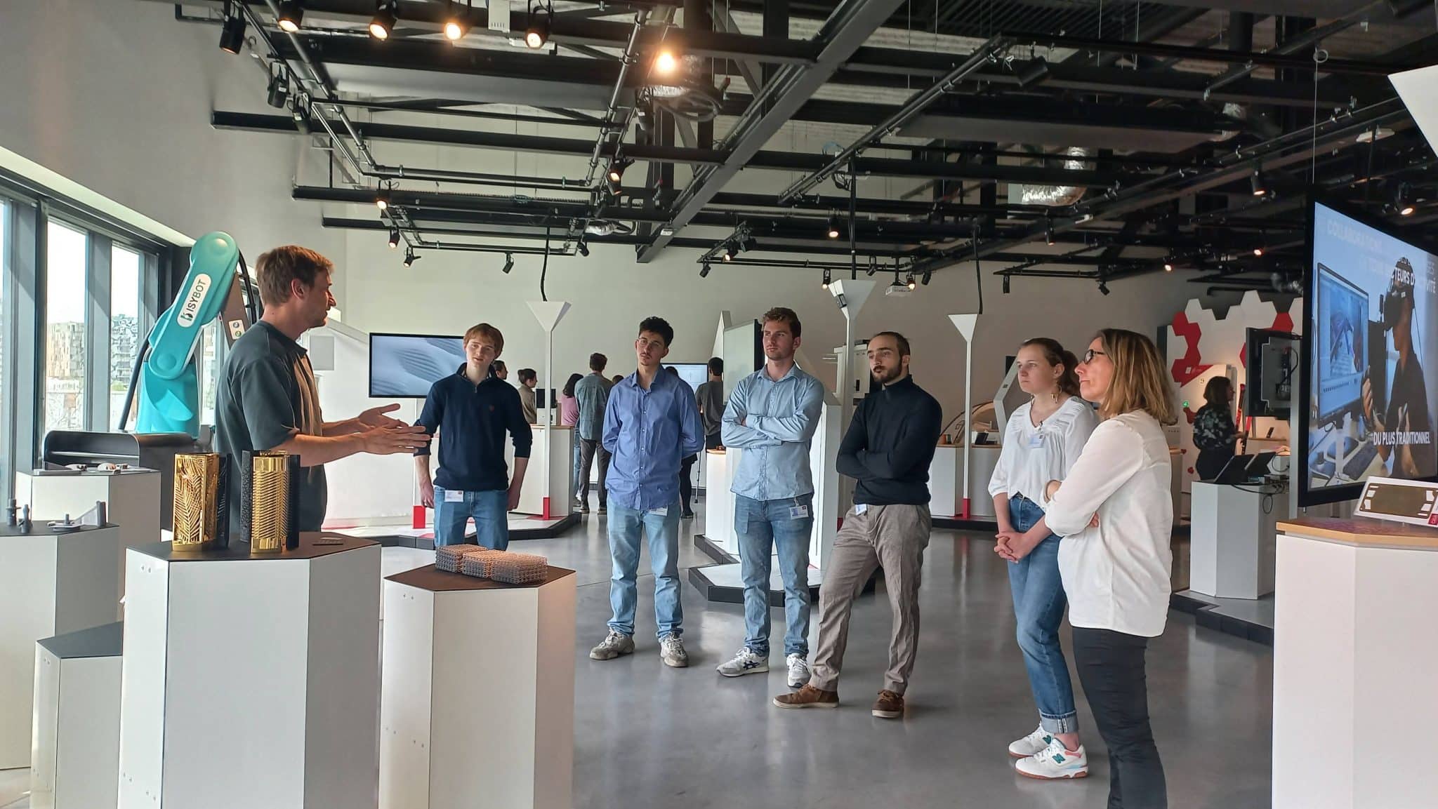
A rewarding afternoon with future engineers from Grenoble INP - Ense3
Read more »
Grenoble, April 4, 2024 - The CEA's Technological Research Division (DRT) welcomed ENSE3 students for an immersive day, revealing the [...].

CEA back in the Top 100 Global Innovators
Read more »
The CEA has once again distinguished itself in Clarivate's TOP 100 Global Innovators 2024, ranking 31st and marking its 12th [...].

